
 芯荃微QW2674A/E LED手电驱动芯片
¥0.06
芯荃微QW2674A/E LED手电驱动芯片
¥0.06
- 商品
- 详情
电动工具MOS管 万芯WP30H100 低压MOS供应商 30V100A功率管
- ¥0.01 1000000 - 99999
- ¥0.03 100000 - 9999
- ¥0.05 ≥10000
参数
- 万芯品牌
- WP30H100型号
- PDFN5x6封装
广东 深圳
3天内发货
100000000
芯荃微QW2674A/E LED手电驱动芯片
¥0.06
产品详情
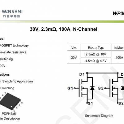
WP30H100
30V, 2.3mΩ, 100A, N-Channel
1.Features
◆ 30V MOSFET technology
◆ Low on-state resistance
◆ Fast switching
◆ Vgs±20V
2.Applications
◆ Power Switching Application
◆ Load Switching
PDFN5x6
Pin Description
VDS
RDS(on) Typ.
ID Max.
30V
2.3mΩ @ 10V
100A
4.5mΩ @ 4.5V
Schematic Diagram
3.Absolute Max Ratings at Ta=25℃ (Note1)
Parameter
Symbol
Maximum
Units
Drain to Source Voltage
VDSS
30
V
Gate to Source Voltage
VGSS
±20
V
Drain Current (DC)
ID
100
A
Drain Current (Pulse), PW≤300μs
IDP
270
A
Total Dissipation
PD
38
W
Avalanche Energy, Single Pulsed
EAS
185
mJ
Junction Temperature
Tj
150
℃
Storage Temperature
Tstg
-55 to +150
℃
Note 1: Stresses exceeding those listed in the Maximum Ratings table may damage the device. If any of
these limits are exceeded, device functionality should not be assumed, damage may occur and reliability may
be affected.
4.Thermal Resistance Ratings
Parameter
Symbol
Value
Unit
Junction to case
RθJC
3.2
℃/W
Note 2:When mounted on 1 inch square copper board t ≤ 10sec The value in any given application depends
on the user's specific board design.
Rev.0.5 WAN SEMICONDUCTOR (NINGBO) CO.,LTD 2
WP30H100
5.Electrical Characteristics at Ta=25℃ (Note 3)
Parameter
Symbol
Test Conditions
Min.
Typ.
Max.
Units
Drain to Source Breakdown Voltage
V(BR)DSS
ID = 250μA, VGS = 0V
30
V
Zero-Gate Voltage Drain Current
IDSS
VDS = 30V, VGS = 0V
1
μA
Gate to Source Leakage Current
IGSS1
VGS = ±20V, VSS = 0V
±100
nA
Gate Threshold Voltage
VGS(th)
VDS=VGS, IDS=250μA
1.0
1.5
2.5
V
Static Drain to Source On-State
Resistance
RDS(on)
ID = 20A, VGS = 10V
-
2.3
4
mΩ
ID = 10A, VGS = 4.5V
-
4.5
6
mΩ
Input Capacitance
Ciss
VGS=0V,
VDS=15V,
Frequency=1.0MHz
3500
pF
Output Capacitance
Coss
500
pF
Reverse Transfer Capacitance
Crss
431
pF
Turn-on Delay Time
td(on)
VDD = 15V, ID = 30A,
VGS = 10V,
RGEN = 3Ω
26
ns
Rise Time
tr
24
ns
Turn-off Delay Time
td(off)
91
ns
Fall Time
tf
39
ns
Total Gate Charge
Qg
VDS = 15V,
VGS = 10V,
IDS = 30A
38
nC
Qgs
9
nC
Qgd
13
nC
Diode Forward Voltage
VFSD
IS = 30A, VGS = 0
1.2
V
Note 3:Product parametric performance is indicated in the Electrical Characteristics for the listed test
conditions, unless otherwise noted. Product performance may not be indicated by the Electrical
Characteristics if operated under different conditions.
Rev.0.5 WAN SEMICONDUCTOR (NINGBO) CO.,LTD 3
WP30H100
6.Typical electrical and thermal characteristics
Output Characteristics Typical Transfer Characteristics
On-resistance vs. Drain Current Body Diode Characteristics
Gate Charge Characteristics Capacitance Characteristics
Rev.0.5 WAN SEMICONDUCTOR (NINGBO) CO.,LTD 4
WP30H100
Normalized Breakdown Voltage vs. Junction Temperature Normalized on Resistance vs. Junction Temperature
Safe Operating Area Continuous Drain Current vs. Case Temperature
Maximum Effective Transient Thermal Impedance
Rev.0.5 WAN SEMICONDUCTOR (NINGBO) CO.,LTD 5
WP30H100
7.Package Dimensions
Rev.0.5 WAN SEMICONDUCTOR (NINGBO) CO.,LTD 6
WP30H100
8. Important Notice
WAN SEMICONDUCTOR (NINGBO) CO.,LTD reserves the right to make corrections, enhancements,
improvements and other changes to its semiconductor products and services and to discontinue any product
or service. Buyers should obtain the latest relevant information before placing orders and should verify that
such information is current and complete. All semiconductor products (also referred to herein as
“components”) are sold subject to WANSEMI’s terms and conditions of sale supplied at the time of order
acknowledgment.
WANSEMI warrants performance of its components to the specifications applicable at the time of sale, in
accordance with the warranty in WANSEMI’s terms and conditions of sale of semiconductor products. Testing
and other quality control techniques are used to the extent WANSEMI deems necessary to support this
warranty. Except where mandated by applicable law, testing of all parameters of each component is not
necessarily performed.
WANSEMI assumes no liability for applications assistance or the design of Buyers’ products. Buyers are
responsible for their products and applications using WANSEMI components. To minimize the risks
associated with Buyers’ products and applications, Buyers should provide adequate design and operating
safeguards.
No WANSEMI components are authorized for use in FDA Class III (or similar life-critical medical
equipment) unless authorized officers of the parties have executed a special agreement specifically governing
such use.
Unless WANSEMI has specifically designated certain components which meet ISO/TS16949
requirements, mainly for automotive use, WANSEMI will not be responsible for any failure of such
components to meet such requirements.
为您推荐
 在线问
在线问
产品参数
- 万芯
- WP30H100
- PDFN5x6
- 新
- 详情见规格书
- 详情见规格书
- 详情见规格书
- 详情见规格书
- 详情见规格书
- 详情见规格书
- 详情见规格书
- 详情见规格书mW
- 详情见规格书
- 详情见规格书
- 详情见规格书
