产品标题: AB 1747-L552中文PDF工业键盘说明书在线阅读
型号:AB 1747-L552
质保:七天验收期,质保期一年
品牌:AB
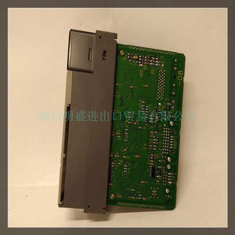
产品图片展示

产品详情资料:
在第4.4节的编程示例中,所有16个DAC在即时更新模式下加载了满标度值FFFH。为了便于说明,本编程示例将通过使用延迟DAC更新模式获得相同的结果。延迟DAC模式可跳线选择,如第5.7节所述。图4.6-1中的流程图显示了编程顺序和示例程序列表,注释如图4.6-2所示。假设基址为FF0060H。在下面的程序示例中,所有16个DAC通道都加载了新数据,然后在程序控制下更新。或者,如果之前启用,外部触发器输入可能已启动DA转换过程。
1.将寄存器D0(用作计数器)初始化为0.2.加载控制寄存器(D15必须为1),以启用P3连接器的模拟输出。3.将DAC通道1的地址加载到地址寄存器A0 4中。用值加载DAC通道。地址指针自动递增到下一个DAC通道。5.存储在D0.6中的增量计数器。如果尚未加载所有16个DAC通道,则转至步骤7.7。加载下一个DAC信道。8.停止
产品英文详情资料:
In the programming example in Section 4.4, all 16 DACs were loaded with a full scale value of FFFH in the immediate update mode. For illustration purposes, the same result will be obtained by this programming example by using the delayed DAC update mode. The delayed DAC mode is jumper selectable, as described in Section 5.7. The flow chart in Figure 4.6-1 shows the programming sequence and example program listing, and comments are shown in Figure 4.6-2. A base address of FF0060H is assumed. In the following program example, all 16 DAC channels are loaded with new data then updated under program control. Alternatively, if previously enabled, an external trigger input could have initiated the DA conversion process.
1. Initialize register D0 (used as a counter) to 0. 2. Load control register (D15 must be a 1) to enable analog outputs to P3 connector. 3. Load address of DAC Channel no. 1 into address register A0 4. Load DAC channel with maximum value. Address pointer is automatically incremented to next DAC channel. 5. Increment counter stored in D0. 6. If all 16 DAC channels have not been loaded, then go to step 7. 7. Load next DAC channel. 8. STOP