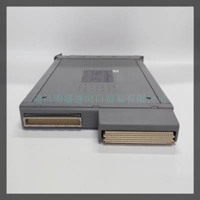
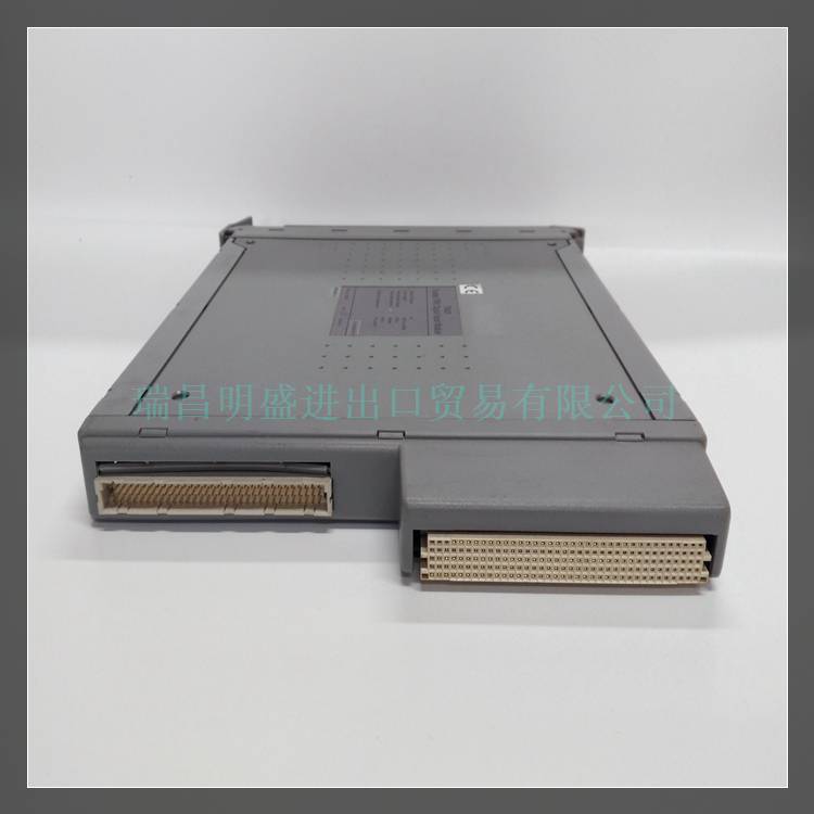
产品标题:ICS TRIPLEX T8403可控硅模块文使用说明
型号:ICS TRIPLEX T840
质保:七天验收期,质保期一年
品牌:ICS TRIPLEX
产品图片展示

产品详情资料:
数模转换器(DAC)板内存映射在短I/O地址空间中。该板在65535字节的VME短I/O地址空间中占据16个连续的字位置。短I/O空间位于FF0000 HEX到FFFFFF HEX之间。由于DAC输出分辨率为12位,因此每个写入或读取周期必须是一个字传输到偶数地址。板基址(XXXXX 0 HEX)可由DIP开关选择,如第5.5节所示。图4.1-1表示VMIVME-4100地址图,假设工厂设置的基址为FF0000 HEX。请注意,控制状态寄存器(CSR)可以写入电路板占用的任何16个字的位置,也可以从中读取。当写入电路板时,数据的目的地由数据位15控制。如果数据位15是“一”,则字被写入控制寄存器;然而,当数据位15为“零”时,数据被写入被寻址的DAC。读取板上的任何地址都会返回板的状态。有两种类型的寄存器必须写入才能使DAC板正常运行。一个是CSR,另一个是DAC。根据DAC通道启动转换所需的操作模式,它们的写入顺序可能不同。
产品英文详情资料:
The Digital-to-Analog Converter (DAC) Board is memory mapped in the short I/O address space. The board occupies 16 successive word locations in the VME short I/O address space of 65,535 bytes. The short I/O space is located from FF0000 HEX to FFFFFF HEX. Each write or read cycle must be a word transfer to an even address, due to the DAC output resolution of 12 bits. The board base address (XXXXX0 HEX) may be selected by DIP switches, as shown in Section 5.5. Figure 4.1-1 represents the VMIVME-4100 address map, assuming the factory set base address of FF0000 HEX. Note that the Control Status Register (CSR) can be written to and read from any of the 16 word locations that the board occupies. When the board is written to, the destination of the data is controlled by data bit 15. If data bit 15 is a "one", the word is written to the control register; whereas, when data bit 15 is a "zero", the data is written to the DAC which is addressed. Reading any address on the board will return the status of the board.There are two types of registers that must be written to for proper operation of the DAC Board. One is the CSR, the other is the DACs. The order in which they are written to may differ, depending on the desired mode of operation for DAC channel start convert.